
A Zener diode, a type of silicon semiconductor, permits the flow of electric current bidirectionally, both forward and reverse. Occasionally termed as a stabilizer, this component is distinguished by its unique p-n junction, which is heavily doped to facilitate reverse conduction once a specific voltage threshold is surpassed. Contrary to traditional diodes that prevent current flow when the cathode potential exceeds the anode’s, Zener diodes are engineered to initiate conduction in reverse once the applied voltage crosses a predetermined level.

Its crucial parameter is the breakdown voltage of the “p-n junction”. When diode is forward-biased it operates just like a typical semiconductor diode. It means that it starts conducting current after voltage crosses the threshold voltage of this diode (for a silicon diode approx. 0.7V).
Zener Diode – Tasks for students
If you are a student or simply want to learn how to solve Zener Diode tasks, please visit this section of our website where you can find a wide variety of electronic tasks.
What differs Zener diode from regular semiconductor diode is when Zener is reverse-biased, one can notice that Zener diode is able to conduct electricity after exceeding the specified voltage at the junction, so called Zener breakdown voltage without damaging the component. The value for the breakdown voltage is correlated with high constancy and does not vary with changes in reverse current. After exceeding this voltage, current value rapidly increases. For small voltages (up to 5V) Zener effect plays a crucial role. In the range of 5-7V, the Zener effect and avalanche breakdown is the main one. And lastly, and after exceeding 7V – only avalanche breakdown takes place. It is worth mentioning that Zener breakdown occurs in heavily doped junctions, whereas avalanche breakdown in weakly doped. We can assume that the voltage breakdown of the Zener diode is not relevant with the current that flows through the diode (only in cases of large breakdown current changes very slight changes may be noticed – low dynamic resistance)
How the zener diode works
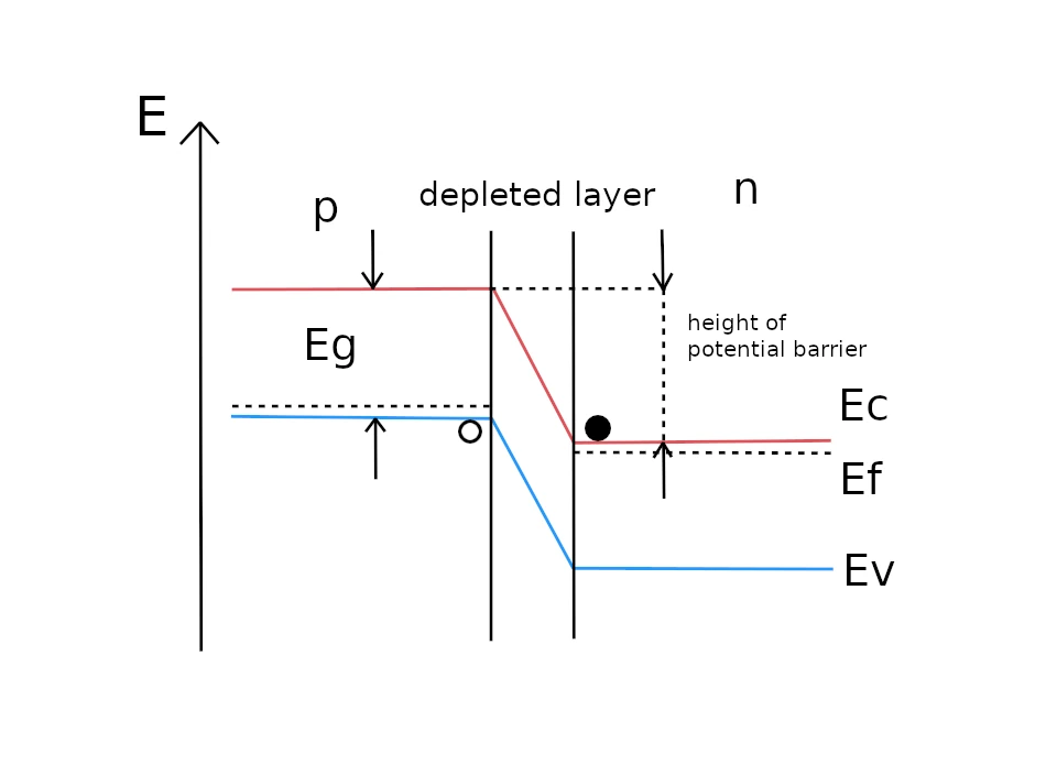
The operation of a Zener diode hinges on two primary processes that lead to the breakdown of its p-n junction: Zener breakdown and avalanche breakdown. These phenomena facilitate the diode’s ability to conduct current in reverse when subjected to a voltage above a specific critical value known as the Zener voltage (UZ).
Zener breakdown is observed in p-n junctions with high doping levels, creating a potent electric field within the slender depletion zone. This intense field can dislodge electrons from their covalent bonds within the semiconductor’s crystal structure, generating electron-hole pairs. This process, in essence, is the electron tunneling from the valence band to the conduction band without energy alteration, facilitated by the p-n junction’s energy band framework. The likelihood of electron tunneling across the junction’s energy barrier increases with a decrease in the barrier’s width and height, making the Zener effect predominant in situations where the junction barrier is both low and narrow.
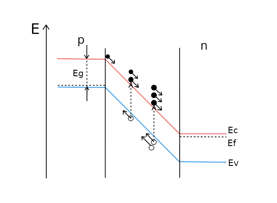
The avalanche effect in Zener diodes is characterized by the exponential multiplication of charge carriers, both electrons and holes, within the depletion zone of the p-n junction. This multiplication results from the interaction between free-moving electrons and the atoms in the semiconductor’s crystal lattice. Collisional ionization, a key aspect of this phenomenon, occurs when a free charge carrier, propelled by a robust electric field, transfers sufficient energy to break the covalent bonds of atoms in the lattice, thereby generating additional free electrons and holes.
As these newly freed carriers are further accelerated by the electric field, they gain enough kinetic energy to initiate further ionization events upon collision, leading to a cascade of charge carrier generation known as the avalanche effect. This process is more likely to occur in p-n junctions that are lightly doped and have a depletion layer thick enough to allow electrons to gain the requisite kinetic energy for successful collisional ionization. Consequently, the electrical current through the junction surges as the number of carriers increases, significantly enhancing the diode’s conductivity in the reverse-biased condition.
Notably, the phenomena of Zener and avalanche breakdown in themselves do not inherently damage the semiconductor device. Provided the external circuit incorporates sufficient current limiting measures, the device can function indefinitely within its breakdown region without harm. The crux of potential damage lies in the absence of current regulation, leading to overheating due to excessive power accumulation within the device, which ultimately results in its failure. Zener diodes are specifically designed to operate safely within a distinct segment of the current-voltage (I-V) characteristic curve, where a sharp rise in reverse current is observed either due to Zener or avalanche effects.
When forward-biased, a Zener diode exhibits typical diode behavior, with a nominal voltage drop ranging between 0.6 to 0.7 volts. In reverse-bias conditions, a precise voltage threshold triggers a dramatic increase in reverse current with minimal voltage fluctuation, a feature harnessed to maintain voltage stability across the device. This voltage regulation capability, irrespective of current flow variations, is a hallmark of Zener diode application. The dominance of the Zener effect is prevalent in highly doped diodes at breakdown voltages between 2 to 5 volts, while avalanche multiplication is characteristic of lightly doped diodes with threshold voltages above 10 volts. Diodes with intermediate doping levels exhibit both breakdown behaviors in the voltage range of 5 to 7 volts.
Zener Diode parameters
You can see the list of main zener diode static and dynamic parameters of this component down below:
Static parameters
- VF – forward voltage at fixed forward current IF,
- IR – reverse current at given VR reverse voltage (most often VR value is 1V)
It should be noted that these parameters may be irrelevant when diode is operating in “breakdown area”.
- VZ – Zener voltage, corresponding to the contractual current value of stability (information available in the data sheets of individual diodes)
- TKVZ – factor temperature of stability voltage (proportion of relative change of stability voltage to the absolute change in ambient temperature at a certain current stabilization).
The resistance rz can also be determined using the static characteristic I(U) at a specific diode stabilization current. The name of such resistance should then be incremental-differential resistance.
Zener diode parameters is characterized by the following limitings:
- IFMAX – the maximum, constant current conduction,
- IFMMAX – peak, permitted current of the diode in forward-biased state (conduction state). Usually given for low and medium power diodes,
- IZMAX – the maximum, permitted current stabilization value, in most cases determined from the quotient of Pad dissipation rate and voltage stabilization Pad VZ,
- PMAX – maximum power loss.

How Zener Diode Regulate Voltage
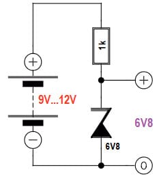
In the depicted stabilization circuit configuration, a resistor R furnishes power to the load, accompanied by a Zener diode D, which is arranged in parallel to the load. The operational principle of the stabilizer exploits the characteristic of the Zener diode’s breakdown voltage VD, which demonstrates a minimal dependency on the diode’s current conduction. Variations in the input voltage VIN or load current I induce fluctuations in the Zener diode current IZ, yet the output voltage VOUT sustains a near-constant level, closely aligning with the Zener breakdown voltage VZ.
The fundamental characteristics of this stabilization mechanism are intrinsically related to the Zener diode’s physical properties, such that the output voltage VOUT is approximately equal to the Zener voltage VZ. Nonetheless, it is imperative to acknowledge that Zener diodes are subject to certain variability in parameters. For the commonly utilized Zener diodes, designated by the suffix C, the tolerance in breakdown voltage can reach up to 5%. This tolerance must be taken into account when implementing Zener diodes in precise voltage stabilization applications.
Minimum current of the Zener diode

Zener diode manufacturers delineate in their catalogs a specified current, termed the nominal current IZ, which is essential for appropriate voltage stabilization. This nominal current IZN is the reference point at which the nominal stabilization voltage VZ and the dynamic resistance of the diode rDZ are ascertained. IZN, therefore, is defined as the threshold current through the Zener diode; below this level, the manufacturer does not guarantee the specified stabilization voltage or the diode’s resistance parameters. It is observed that as the current passing through the Zener diode increases, there is a slight reduction in its dynamic resistance.
For a majority of low-power Zener diodes, a standard value of IZN is designated as 5 mA, as stipulated in product catalogs. However, this figure should not be misconstrued as the absolute minimum current for Zener diode functionality. Modern Zener diodes typically maintain acceptable performance characteristics at currents significantly below 5 mA. Indeed, there are Zener diodes available in the market whose IZN is stated as being around 1 mA in the product specifications.
Moreover, if an integrated voltage stabilizer, which emulates a diode’s behavior, such as the TL 431 or LM 385, is employed in lieu of a Zener diode, the minimum operating current for these devices may be well below 1 mA. In such instances, it is imperative to consult the specific catalog data.
The prescribed method for calculating the IZN current informs the design process of a stabilizer using a Zener diode. When the following parameters are known: the minimum expected input voltage of the stabilizer VINMIN, the nominal diode voltage VZN, and the maximum anticipated load current IOMAX, the resistance value for the resistor R is determined in accordance with the design criteria to ensure proper functionality of the stabilizer circuit.

Stabilization factor
The stabilization factor within a circuit employing a Zener diode is intrinsically linked to the diode’s inherent physical attributes. Within such a framework, the voltage source VZN0 is indicative of the Zener diode’s nominal voltage, whereas the resistor rDZ represents the diode’s dynamic resistance. Given a scenario where there is an incremental change in the input voltage denoted by ΔVIN, coupled with the assumption that the load current IO remains relatively constant (especially when the increment in input voltage is minor), the resultant change in output voltage can be articulated as follows:

From here, the SV stabilization factor of a circuit with a Zener diode can be calculated, which is equal to:

In the context of Zener diode behavior, it is critical to note that the dynamic resistance, denoted as rDZ, is commonly specified in manufacturers’ catalogs based on a standardized nominal current, which is often 5 mA. It is observed that with an increase in the current traversing the Zener diode, the dynamic resistance, rDZ, decreases. Consequently, an enhancement in the stabilization factor of the diode is achieved under these conditions.
The resistance value of rDZ at the catalog nominal current IZ of 5 mA typically spans a range from several ohms to several tens of ohms. However, it is imperative to recognize the potential for significant variability among individual diodes. The dynamic resistance may exhibit substantial variances, potentially extending to tens of percent, between different units of the same type of diodes. This variability must be considered when implementing Zener diodes in circuits where precision is of paramount importance.
Output resistance of the circuit with a Zener diode
The output resistance, of a stabilizer with a Zener diode “seen” from the VOUT voltage side, is:

It merits reiteration that the computation of the output resistance rOUT, as presented in the foregoing equation, holds significance solely when the Zener diode operates within its breakdown state. Within such a state, the Zener diode conducts current due to the breakdown effect, which is characteristic of this component under certain conditions. It is during this phase that the diode’s resistance diminishes considerably. Conversely, if the diode is not in a conducting state—when it is not subject to sufficient voltage to induce breakdown—its inherent resistance is substantially high, resulting in an output resistance of the circuit that is effectively equivalent to the resistance R. This resistance can be excessively large for the requirements of the powered circuit.
With contemporary Zener diodes, it is commonly observed that the resistance R significantly exceeds the dynamic resistance rDZ. Consequently, the output resistance of a well-designed stabilizer circuit incorporating a Zener diode tends to approximate the dynamic resistance rDZ, given that the Zener diode is in a state conducive to current conduction (i.e., in breakdown).
Permissible maximum current of the Zener diode
In the realm of Zener diode specifications, manufacturers typically abstain from detailing the maximum permissible current. Instead, they provide data concerning the maximum tolerable power dissipation (loss) for such diodes. As a result, the maximal current capacity for a specific Zener diode can be deduced by dividing its allowable power dissipation by its breakdown voltage. Employing this formula, let us take the BZX55-C6V2 diode as an illustrative example, which possesses a breakdown voltage VZ of 6.2 V and a maximum power rating PMAX of 0.5 W as specified in the catalog. The maximum current for this Zener diode would thus be calculated accordingly.

However, the actual maximum current, IDMAX, is marginally less than this calculated value. This discrepancy arises because, under conditions of high current flow, the voltage drop across the diode marginally exceeds its nominal voltage, VZ. Hence, to ensure the diode’s integrity, the IDMAX current must be calculated with a margin below the theoretical maximum.
When designing a voltage stabilizer circuit that incorporates a Zener diode, the maximum Zener current, IZMAX, informs the minimal allowable value for the resistor R to be used in the circuit. This value must be determined by considering the highest anticipated input voltage, VINMAX, and the smallest expected load current, IOMIN, that the stabilizer will need to accommodate. This approach ensures that the Zener diode will operate within safe parameters, thus avoiding its destruction due to excessive power dissipation.

It is worth mentioning on this occasion that when the current flowing through a diode increases, its temperature also increases. Since Zener diodes have non-zero temperature coefficients, this causes a thermal – and therefore with a rather long settling time – change in the voltage VZ.
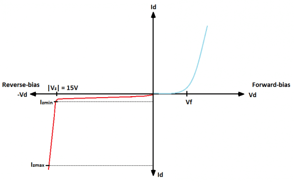
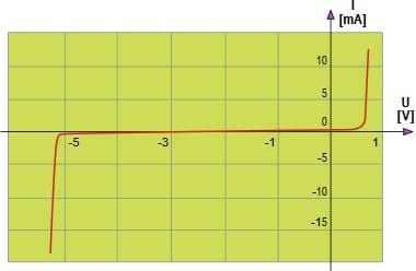
V-I Characteristics of Zener Diode
In the domain of semiconductor devices, the Zener voltage, denoted as VZ, signifies the reverse bias voltage at which a Zener diode’s characteristic response curve undergoes a pronounced shift, indicative of the onset of the breakdown region. The magnitude of VZ is contingent upon the resistivity characteristics of the silicon material constituting the diode. Typically, for the most prevalent Zener diodes, VZ spans a spectrum from several volts up to numerous tens of volts.
Within the breakdown region, the voltage differential, known as the stabilization voltage across the diode, remains largely invariant with respect to the current coursing through the diode. It is the dynamic resistance, symbolized as rZ, that quantifies the stabilization voltage’s sensitivity to variations in current. This parameter is defined by the quotient of a minute increase in the stabilization voltage VZ to a corresponding increment in the current IZ. Thus, rZ provides a metric of how the Zener diode’s voltage stabilization performance is influenced by changes in current flow through the device.

The dynamic resistance of the Zener diode in the stabilization range is very small. In approximate considerations, the stabilization voltage is assumed to be constant (independent of current) equal to the value of Zener voltage VZ. The maximum value of current IZMAX, at which the Zener diode can operate, is limited by its permittivity PTOT according to the relation:

When the PTOT power is exceeded, the diode may fail due to thermal breakdown of the P-N junction.
Forward Characteristics of Zener Diode

Within the operational domain of semiconductor devices, a Zener diode, when biased in the conduction direction, exhibits the characteristics akin to a standard rectifying diode. It remains non-conductive in the forward direction until the applied voltage reaches the threshold known as the Zener voltage. Upon surpassing this specific voltage, the diode transitions to a conductive state. Typically, Zener diodes are employed in their reverse-biased mode, referred to as barrier polarity. The graphical representation associated with the diode illustrates the onset of conductivity at the point where the voltage surpasses the 3.9 V threshold. This operational trait underpins the use of Zener diodes in various applications where voltage regulation or over-voltage protection is required.
Zener Diode Applications
Zener diodes are often used to protect circuits from surges. Their characteristics mean that when a certain voltage is exceeded, this diode begins to conduct, directing excess current out of the circuit and protecting it from damage.
Zener voltage regulator
Voltage stabilization systems are among the most utilized. A few devices are powered with batteries (rechargeable batteries) as well as the output voltage of the power sources may fluctuate within a relatively broad variety.
Let us look at methods to create secure voltages. Obviously, you always have the option to utilize an integrated voltage regulator (IC), however, there are quite a few other intriguing approaches, the majority of which just require several (usually different ) components.
Voltage stabilization isn’t a tricky problem in training as good voltage regulator ICs like the 7805 are easily offered. Because of this, a voltage regulator is commonly utilized in these devices to supply a slightly reduced but steady voltage, like 5V for electronic circuits or to get a microcontroller. When working with an input voltage which range from 7V to 30V, then it offers an output voltage of just 5V. On the other hand, the use of the integrated circuit includes a high number of elements. Alternatively, you can handle 1 semiconductor apparatus, specifically a zener diode. The 7805 stabilizer really comprises a zener diode alongside a significant number of transistors. A zener diode is a sort of diode where a breakdown happens using a well-defined reverse osmosis. The principle of performance of the circuit is a result of the aspects of a common zener diode. The very first breakdown takes place when the reverse voltage rises above a specific value (UZ), which contributes to a sharp gain in the reverse present. The voltage throughout the diode stays stable in the breakdown voltage, so provided that you don’t overdo the opposite current. The next breakdown is a regularly observed disadvantage when using zener diodes. In the event the zener diode gets too hot, then the junction will short-circuit, and following this occasion that the diode elevates the voltage in a level near zero. Simply speaking, the expression zener diode isn’t necessarily appropriate as two distinct phenomena are responsible for its breakdown impact at voltages which range from 3V to 200V. It’s a negative temperature coefficient, inducing the zener voltage to fall to 0.1percent per level. The avalanche impact that overlooks over 5.6V comes with a positive temperature coefficient.
How to test Zener Diode

To ascertain the functional integrity of a Zener diode, the initial step involves configuring a multimeter to its diode testing mode. Upon connecting the multimeter’s probes to the diode’s terminals—specifically, attaching the red probe to the anode and the black probe to the cathode—a typical reading should display a value in the range of several hundred millivolts. Conversely, when the probes’ orientation is reversed, the multimeter is expected to indicate a reading that exceeds the measurement range.
Should the multimeter yield identical readings in both orientations, this serves as an indication of a malfunctioning diode. The subsequent phase of testing involves the utilization of a DC voltage supply to further examine the Zener diode, which is connected in its reverse-biased orientation. Concurrently, a DC voltmeter is connected in parallel to the diode for voltage monitoring purposes. Gradually increasing the output voltage of the power supply, a properly functioning Zener diode, designated with a Zener voltage of 9.1V, is characterized by its inability to conduct in reverse until the applied voltage surpasses the specified Zener voltage threshold. If the diode commences reverse conduction at a voltage lower than its rated Zener voltage, this condition suggests impairment, necessitating the replacement of the component.