
Organic LED
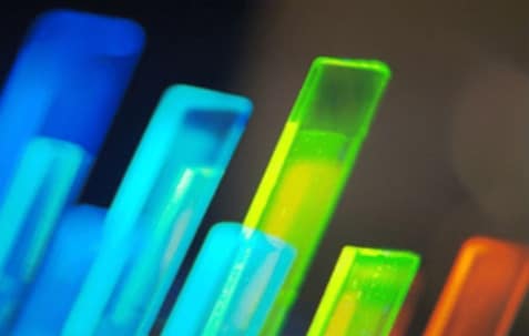
OLED (Organic LED) – the type of light emitting semiconductor diode that is used as a superficial light source. They are used to build flexible displays, TVs or other portable devices. Displays produced in OLED technology are extremely thin due to the lack of need for their backlighting, because they generate light by itself. OLED technology will undoubtedly „take the torch” from the LCD technology. OLED symbol looks the same as a typical LED’s.
OLED – Internal construction and manufacturing process
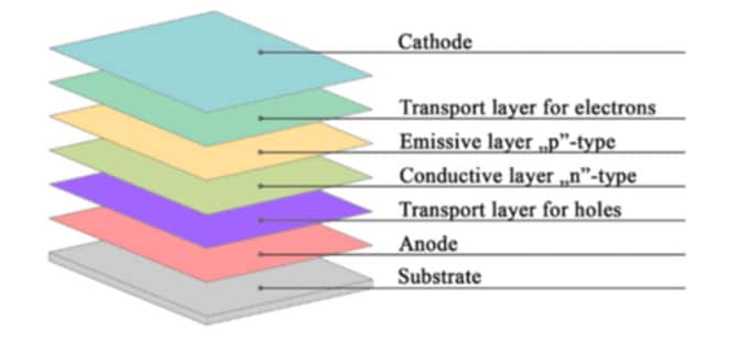
Organic LED is constructed from several very thin layers of materials put on-top of each other in a way that is „similar to the sandwich”. These layers are as follows:
- two conductive electrodes:
- anode (+) – transparent, to make the passage for the emitted light (also known as „emitter”),
- cathode (-) – not necessarily transparent (also called „conductor”),
- two organic layers:
- conductive layer – “n” -type organic semiconductor,
- emissive layer – “p”-type organic semiconductor, here applied organic material is different than on the conductive layer, the layer is so-called because it emits electromagnetic radiation in the visible spectrum. Therefore, this layer is called emissive,
- base – transparent, usually made from glass or foil.
It is possible to “add” a third organic layer for a more efficient transfer of electrons from the cathode to the emissive layer.
Technological process of OLEDs is usually done in the following order:
- The substrate is applied to the anode.
- The layer on the anode is formed especially for the transport of holes.
- Application of the conductive layer “n” -type.
- The layer is placed on-top of the conductive layer to form emissive “p” –type layer.
- Next, the transport layer for electrons is applied.
- The cathode is „placed on-top of everything”.
The thickness of the layers in the OLED technology does not exceed 500nm.
Organic LED Principle of operation
The most important thing in OLED operation is applying the correct voltage to its structure for the light emission to be possible and successful. The electrons move in the direction from cathode to anode (electrons from the cathode pass into the emissive layer and holes will pass from anode, which means that anode will retrieve electrons from the conductive layer). Once the junction is forward-biased, the emissive layer is negatively charged. However, the conductive layer is positively charged because of the presence of excess holes that are a positive charge-carriers. The mutual attraction of electrons and holes in the emissive layer arises due to the occurrence of electrostatic interaction. Then the recombination phenomenon occurs – connection of a pair of particles with opposite electrical charges. The energy released during recombination causes the emission of visible electromagnetic radiation – light. Value of the voltage that supplies OLEDs (the bigger, the brighter means larger OLED power consumption) defines the brightness of the received light. The color of this light depends on the type of the organic layer of material used in an emissive layer in the OLED technology. It will be lit only when the junction is forward-biased (reverse-bias won’t work – just like in typical semiconductor diode).
Organic LED History
Organic LED (OLED) are surface source of lights in which the density of the active layers – polymers – normally is not above 500 nm. The phenomenon of electroluminescence in organic materials was first observed in 1950 by the Frenchman André Bernanose, that, along with his coworkers from the University of Nancy, noticed a faint radiance of the layer of organic material (acridine by-product – acridine orange) after using high alternating voltage (AC) to it. In one more organic material, in 1963, electroluminescence was observed by Martin Pope. The electroluminescence in polymer films was first found by Roger Partridge at the National Physical Laboratory in Great Britain. The structure examined by him included a polymer layer (n-vinylcarbazole) with a density of 2.2 micrometers, which was located between two metal electrodes with a voltage applied to them. The described framework was patented in 1975 and also the results of his research were published in 1983. The very first discoveries of electroluminescence in organic products and also research study carried out in the 1960s and also 1970s did not bode well for their use in practice. This scenario transformed after the magazines of Ching W. Tango as well as Steven Van Slyke. In the 1990s, several lab announced that they had actually handled to obtain a radiance result in a phosphor made of organic materials, similar to that discovered in electroluminescent devices, and that a display prototype had been built on their basis. Among the very first organic compounds to uncover the sensation of light exhaust under the influence of an outside electrical field was polyphenylene vinyl. It turned out that this conductive polymer can give off green or yellow-green light under the influence of applied voltage. The very first working monochrome OLED display showed up in 1996 thanks to Cambridge Display Technology. During that time, this design left a lot to be preferred, particularly when it emerges effectiveness. Only in 1998, organic, green OLEDs were established, which were defined by enough performance in transforming electrical energy right into light. The fast growth of OLED innovation goes back to 2000, when the Taiwanese company RiTEK Display Technology started constructing the first manufacturing facility to generate black and white, glowing green SMOLED screens for smart phones. In 2002, the initial AMOLED (Active Matrix OLED) panels with an energetic control matrix, developed by Kodak, appeared. In October 2007, Sony introduced a model of a TV made in OLED innovation.
Flexible oleds FOLED
FOLED has an electroluminescent layer applied to a flexible substrate. Because of this, the sturdiness of these units is not high in the meantime, due to the fact that the problem is the infiltration of oxygen and water vapor particles through the flexible substratum and also the degradation of the energetic layer. A plastic substratum does not protect like glass, for that reason, in order to enhance the life span of the tools, the seal should be created as well as boosted both in the substratum as well as in the securing film.
There are a number of securing technologies to boost the gas barrier as well as are suitable for Flexible OLED screens. One of them is Dam-and-fill modern technology. Throughout this process, the spread, high-viscosity fluid develops a rectangular barrier around the OLED. This liquid is dispersed during the droplet application operation so regarding fill up the room in between the substratum and also the securing film within the dam. This technique is characterized by simplicity and high security.
Another approach is securing with a thin multilayer film (Thin-film-encapsulation, TFE). TFE modern technology showed the best securing properties for both the Water Distribution Index (WVTR) and also the Oxygen Distribution Index (OTR). The most preferred TFE innovations are chemical plasma vapor deposition (PECVD) as well as atomic layer deposition (ALD).
PECVD (Plasma-enhanced chemical vapor deposition) is a variant of the CVD method that can be made use of to prepare a multi-layer inorganic-inorganic or organic-organic obstacle. Silicon nitride and also silicon dioxide are frequently utilized for this purpose.
PEVCD is an extremely appealing method due to the low procedure temperature (below 600 ° C), the possibility of deposition of non-equilibrium stages and the wonderful control over the sanitation of the coverings.
ALD (Atomic Layer Deposition) is another method that can be used for incredibly exact deposition of a sealing film. Some nitrides and oxides transferred by this approach, e.g. aluminum oxide, have actually been examined for the gas barrier of the plastic film, providing good cause terms of resistance. The disadvantage of this method is the high price of the makers as well as the lengthy process time.
One more means to enhance the gas barrier and also secure the FOLED display is to make use of ultra-thin steel and also glass aluminum foil. Ultra-thin glass (<100 mm) and also steel foils have good impermeability homes. However, such films have the disadvantage of being opaque and also boring and also being quickly harmed.
The last possible modern technology is the so-called FSE (Face-sealencapsulation). The FSE innovation uses sealing films with a low WVTR (Water Vapor Transmission Rate) index. It is a straightforward as well as cheap approach that can be utilized in automation of FOLED screens.
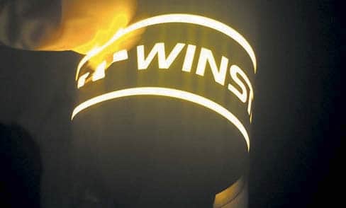
Winstar flexible OLED technology
Winstar’s Flexible OLED display screens are sealed with FSE innovation as displayed in Figure 3. The substrates utilized were a polyamide covered film with a deposition barrier used by PECVD, resulting in a WVTR of 5 · 10-5 g/ day/ cm. A thick 100 nm anode has been topped the seal layer and the Tvis of this barrier is above 85%.
A standard photolithography process is done on the flexible substratum mentioned earlier to produce a shaped insulator. The organic layers as well as metal cathodes are vapor deposited. Finally, the PET-structure securing tape, the securing layer and the pressure-sensitive adhesive are laminated flooring in a procedure called roll-to-sheet. Figure 3 shows a model of such a FOLED display screen.
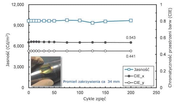
Figure 4 shows the results of tests for repeatable and dynamic flexing of the Flexible OLEDs screen (red color, pixel size 2 × 2 mm) on a span of curvature of approx. 34 mm. The illumination and also the CIE color area (shade scheme) did not change significantly even after 200 cycles. The illumination change aspect is less than 3.08% (<300 cd/ m ²).
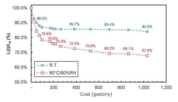
The life time examination was done under normal environmental conditions (22-25 ° C, 30-60% RH) and also high temperature and humidity (60 ° C, 90% RH). In the tool operating at room temperature, illumination after 1000 h was 84% of the first worth. On the other hand, the device operating in high temperature and moisture problems at the same operating time attained a brightness of only 67.9%. The estimated service life mores than 13,000 hours.
OLED – Advantages and disadvantages
The use of OLED technology in the construction of any display has both advantages and disadvantages.
As OLED advantages we can put:
- the possibility of producing flexible displays or sewn-screens e.g. in clothing due to the possibility of applying the organic material on a flexible substrate,
- low weight and thickness of the display,
- reduced manufacturing costs due to the lack of backlighting, non-complex construction (small number of electronic components) and fewer layers of the display,
- OLED meaning greater brightness and color scale than in LCD technology what’s caused by spontaneous, unfiltered light emission by OLEDs,
- the backlight is not required what leads to low OLED power consumption – black color is perfectly black,
- viewing angle is almost unlimited,
- faster response time (~ 0,01ms) compared to LCD technology (2-12ms).
Among OLED disadvantages one can find:
- the lifespan of organic materials – blue OLED has the shortest lifetime among the RGB colors (Red, Green, Blue): about 5000-14000h. However, red and green OLEDs could work between 46,000-230,000h, so blue OLED challenges today’s world of scientists,
- consumption of current – scientists have observed greater power consumption when displaying white and bright elements e.g. while browsing Web, therefore it may be uneconomical for some applications,
- susceptibility to environmental factors – organic materials are particularly sensitive to environmental factors. In case of mechanical damage to the matrix display, water or humidity can easily destroy organic material. Using an additional superficial protection could be a smart idea,
- limited patents – the development of OLED technology is heavily dependent on companies that have ownership of patents (now Eastman Kodak Company), which require the payment of license-fees to allow taking any „serious, further steps” in this subject.
 is the type of Semiconductor Diode, made from organic materials and has the ability of emitting the light. Find out more in this article.)