Lowering your losses
The demand for power on a global basis continues to increase. Estimates put the total power required in 2020 at 30 Petawatts. Efforts to produce more of that power from renewable sources continue, reducing our dependence on fossil fuels. Wherever the power comes from, it is imperative that we use it well, with the highest possible level of efficiency. This not only keeps the cost of power under control, but also our impact on the environment.
Around half of the energy produced worldwide goes into the Industrial sector, predominantly to drive electric motors. However, the 21st Century has brought with it a significant shift towards big energy consumers in the form of data centres. Also, we haven’t really begun to consider how the wholescale shift towards electric vehicles will impact our total energy requirements but suffice it to say it will be significant.
The burden of increasing efficiency falls on the entire power chain, from source to destination. This article will focus on how Wide Bandgap (WBG) semiconductor technology fits into the power landscape.
The Conversion Challenge
The need for power conversion now extends to AC-to-DC, DC-to-DC and DC-to-AC. Every conversion process incurs losses, some applications may need galvanic isolation, while the difference between input and output power will also influence design choices. However, in all instances, one topology has become prevalent: the switched mode power converter.
Early examples of power conversion circuits would have been based on BJT (Bipolar Junction Transistor) technology and its use is still common in various configurations designed to handle high power requirements, such IGBT. However, more recently, MOSFET technology has displaced BJT and in some cases IGBT, but the underlying platform is still ‘plain old’ silicon. The latest developments in the substrate technology employ a different platform based on Wide Bandgap (WBG) substrates. The two most common are Silicon Carbide (SiC) and Gallium Nitride (GaN).
Thanks to their relatively higher efficiency, WBG semiconductors are now being selected for power conversion, particularly in resonant topologies and three-phase bridges as used in motor drive circuits. However, all switching devices feature a conduction path and this path will always incur resistance. This resistance, RDS(ON), will result in losses based on the amount of resistance in the channel and the current flowing through it. Figure 1 illustrates the type of instantaneous voltages and power that a MOSFET may be subjected to when switching.

The losses associated with the on-resistance of a switching device are proportional to the number of times it switches in any given time. It follows, therefore, that low frequency switching results in lower losses. Engineers will appreciate, however, that high-frequency switching circuits can make use of smaller passive, such as capacitors and inductors. Higher switching frequencies in the MHz are attractive for this reason, particularly in applications where power density is a driver. This includes DC-DC conversion in HPC, data centres, and cellular base stations.
A main area of loss in power switching applications is the energy required to overcome the device’s capacitance when charging and discharging. These are referred to EOSS and COSS, respectively, which represents the product of the capacitance between the drain and source, and gate and drain. Together with RDS(ON), EOSS and COSS are critical to overall efficiency. Another metric, RDS(ON)A, takes into consideration the area of the channel based on the physical size of the die. This is also used as a Figure of Merit (FoM) when calculating total losses. It is significant because output capacitances reduce as the die shrinks, but a smaller die tends to increase channel resistance.
How Wide Bandgap semiconductors meet the need
A wide bandgap material needs more energy to get electrons to move from the valence band to the conduction band. As a result, WBG semiconductors have a higher critical breakdown voltage and feature subsequently lower leakage current than silicon devices. These benefits become even more impactful at high operating temperatures. In addition, the electron saturation velocity in WBG devices is also higher, which means faster switching when compared to silicon devices. Figure 2 compares silicon, SiC and GaN in these terms.

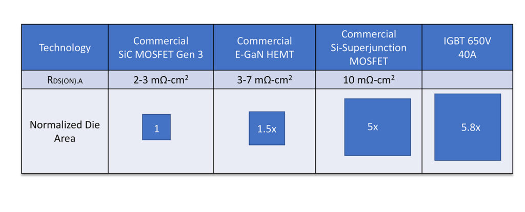
What this means in practice is that a SiC device can be manufactured with a drift layer that is as little as 1 tenth the thickness of a silicon device, but have 10 times the doping. This is only possible due to the higher breakdown voltage. It also results in lower on-resistance and, as demonstrated earlier, lower losses (power dissipation) for the same die area. Because SiC has much higher thermal conductivity, the die can be much smaller with respect to silicon, giving a lot better RDS(ON)A. Figure 3 shows how the FoM of RDS(ON)A compares between a MOSFET, IGBT, SiC MOSFET and GaN HEMT (High Electron-Mobility Transistor).

Another important factor to appreciate is that SiC and GaN devices need much lower gate drive than Si MOSFETs and IGBTs, both of which need very high gate charge in order to switch efficiently. For high power IGBTs, this gate charge can be significant and contributes to the overall losses. Conversely, even at high switching frequencies the gate drive required for WBG devices is much smaller, in the region of milliwatts.
Other reasons why WBG is gaining attention include its ability to operate at temperatures as high as 500°C. In fact, the limitation on operating temperatures is more likely to be set by the packaging technology available, rather than the capability of the die. Importantly, changes in operating temperature do not lead to big variations in on-resistance or leakage.
Key technology developments
While it is true that the cost of WBG devices has been higher than a silicon-based solution, the industry is working hard to address this. But in many applications the value that WBG brings is worth the higher price. The value can be measured in terms of higher efficiency, but that also brings system-level gains, such as higher power density. Another benefit is that WBG devices have simpler heatsinking requirements. And, as covered earlier, the associated passives will also be smaller and lower cost.
Faster switching also delivers benefits at the application level. For example, a faster response time to changes in electric motor loads will result in higher overall efficiency, as well as smoother operation. This would prolong the lifetime of the electric motor and provide improved functionality.
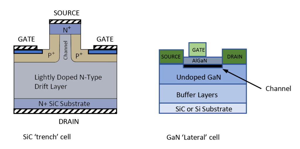
A growing number of manufacturers are now delivering on the promise of WBG. As shown in Figure 4, Infineon has opted for a trench design. Its GaN HEMT devices feature a planar construction which, unlike SiC MOSFETs, have no intrinsic body diode. This makes them suitable for ‘hard switching’ applications.

With a rating of 200°C for its 1200V SiC MOSFETs, STMicroelectronics can claim the industry’s highest operating temperature. This comes with very low on-resistance and robust body diode which can be useful where commutation is present, such as motor drive applications.
Other SiC MOSFETs now available include products from ROHM. Its value proposition includes putting an anti-parallel SiCSchottky barrier diode in the same package, again aimed at commutating applications. The low forward-voltage drop of the Schottky, 1.3V, provides lower losses than the body diode (4.6V).
GaN Systems is also working on WBG solutions, with a focus on packaging technology. This is intended to help engineers access the full benefits of GaN, as outlined earlier. The company’s Island Technology combines a matrix of HEMTs with metal bars to keep resistance and inductance as low as possible. Another packaging technology, GaNPX, removes wirebonding to give the best thermal conductance, leading to higher current density in a small outline.
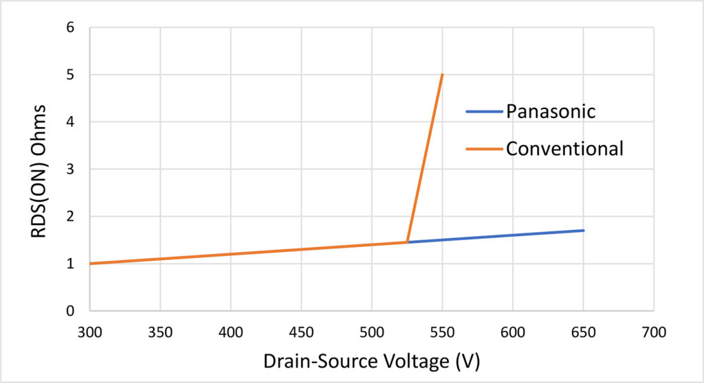
Also working withGaN, Panasonic has developed the X-GaN to address a specific condition known as current collapse. This occurs when trapped electrons between the drain and source can cause the on-resistance to increase. This could potentially lead to failure, as shown in Figure 5. The Gate Injection Transistor developed by Panasonic results in a device that is truly ‘normally off’ but can still use gate drive technology that is compatible with Si MOSFETs.

Conclusion
When looked at objectively, WBG outperforms silicon in almost every metric. While cost may still be a major challenge, that is being addressed. The relatively limited amount of reliability data available may also concern some customers but, again, manufacturers are actively addressing this.
Mouser is now stocking and supplying a wide range of SiC and GaN WBG solutions and associated gate drivers, along with the passive components required to return higher efficiency in your next power switching application.


