
USB technology has progressed– from an information user interface capable of providing minimal power to a main source of power with an interactive information interface. Today, several devices bill or get their power from USB ports had in laptops, autos, aircrafts and even wall sockets.
Because of its small dimension and capacity to both deliver power and transfer data, USB Power Distribution (PD) has actually become a common power outlet for many tiny gadgets such as cellphones, laptops as well as various other handheld gadgets, as displayed in Figure 1.

Figure 1: Instance laptop docking station with USB PD
USB PD specs define just how USB devices can bargain for more existing and/or higher or lower voltages over a USB cable, utilizing the USB Type-C CC wire as the communications channel. USB PD specs allow gadgets with better power demands to get the power they need to operate from the bus voltage (VBUS) while negotiating with outside power sources.
To assist in optimum charging, a USB PD battery charger have to utilize among these two devices:
A listing of fixed voltages, each with its own maximum current.
A listing of programmable voltage ranges, each with a maximum present (programmable power supply), where the gadget will ask for a voltage (in 20-mV increments) that is within the specified range as well as within the optimum existing allowance.
In this post, I’ll show you just how to enhance USB PD billing capacities by including a buck-boost converter to your layout.
Reducing your total design impact while delivering optimum charging efficiency
Concurrent buck-boost converters can convert a battery voltage or adapter voltage right into power-supply rails. TI’s TPS55288, for instance, can readjust the output power array from around 10 W to 100 W based upon the input voltage. Via the I2C interface, the output voltage of the TPS55288 is programmable from 0.8 V to 21.26 V with a 20-mV step. The default result voltage is 5 V when the device is made it possible for, as well as can be used in a docking terminal, vehicle battery charger, cordless charger or PC applications.
Figure 2 shows the service size of the TPS55288 400-kHz examination module board. When operating in increase setting, the TPS55288 can provide 100 W from a 9-V input with a 400-kHz operating frequency.
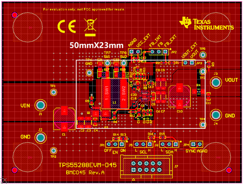
Figure 2: 400-kHz EVM board option size for the TPS55288
Figure 3 shows the conversion performance of the TPS55288 400-kHz EVM board in forced pulse-width inflection (FPWM) setting. When VIN ≥ 12 V, the conversion effectiveness is greater than 95% at the 100-W outcome problem.
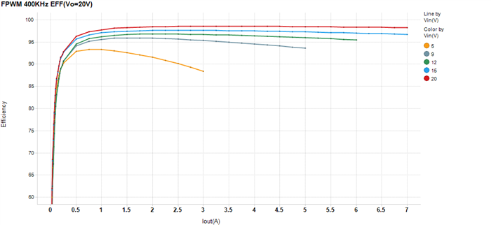
Figure 3: Efficiency vs. result current (fSW = 400 kHz, VOUT = 20 V).
Figure 4 reveals the option size of the TPS55288 2-MHz EVM board. When working in boost setting, the TPS55288 can deliver 60 W from a 12-V input with a 2-MHz operating regularity.
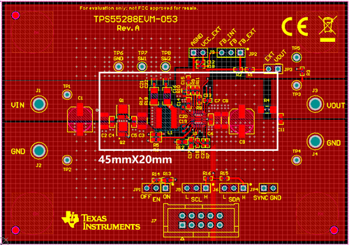
Figure 4: 2-MHz EVM board option size for the TPS55288.
Figure 5 shows the conversion effectiveness of the TPS55288 2-MHz EVM board in FPWM setting. When VIN ≥ 12 V, the conversion performance is higher than 90% at the 60-W output problem.
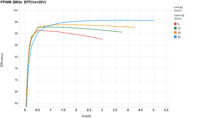
Figure 5: Performance vs. output existing (fSW = 2 MHz, VOUT = 20 V).
Improving thermal efficiency.
Great thermal efficiency suggests greater reliability and also longer lifetime for an item. Figure 6 is a thermal picture of the TPS55288 400-kHz EVM board at 20-V/3-An and 20-V/5-A tons conditions, respectively. The TPS55288 has only a modest 40 ° C temperature increase at a 20-V/3-A lots. Even at 100 W outcome power without a warmth sink or thermal pad, the maximum temperature level on the TPS55288 is just 86.4 ° C, a lot lower than the 150 ° C limit.
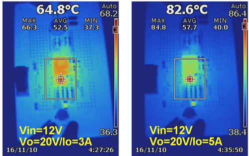
Figure 6: Thermal performance (fSW = 400 kHz).
Attaining low EMI.
An essential design obstacle for the power supply style is passing the electromagnetic disturbance (EMI) examination. Circuits that fall short the EMI test repeatedly usually need round-the-clock initiatives in the laboratory to stay clear of and fix the problem item launch delays. The TPS55288 buck-boost converter can achieve excellent EMI efficiency. With regularity dithering feature and by transmitting and also optimizing the positioning, the device can pass CISPR25 degree 5 performed discharge as well as radiated emission limitations, which are really rigorous.
Figures 7 and 8 reveal the EMI performance of the TPS55288 buck-boost converter under 400-kHz as well as 2-MHz operating frequencies, respectively. The test result passes the CISPR 25 level 5 limit with greater than 6 dB margin.
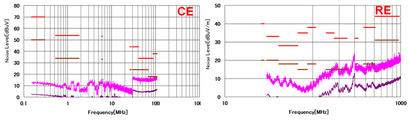
Figure 7: Performed as well as radiated EMI results under fSW = 400 kHz (12 VIN, 15 VOUT/3 A).
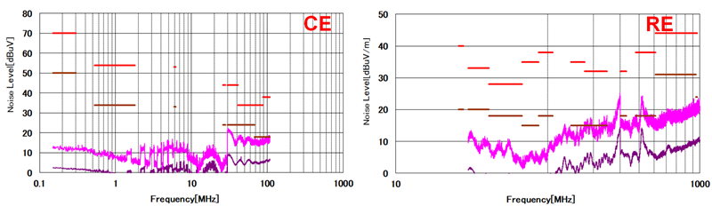
Figure 8: Carried out and also emitted EMI results under fSW = 2 MHz (12 VIN, 15 VOUT/3 A).
Benefits of a programmable outcome current-limit feature.
High efficiency, small option size as well as reduced EMI, other attributes make the TPS55288 a good fit for USB PD applications.
The TPS55288 buck-boost converter can configure the output current-limit factor, which aids the circuit easily pass the UL 100-W maximum result power test. If the output existing exceeds the collection output existing limit, you can use the 03H internal register to set the feedback delay time. This enables the TPS55288 to output high existing in a fairly short time, which helps the circuit meet the optimal existing requirement in Section 6.4.1 of the USB PD specification.